
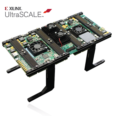
ASIC Prototyping System
Technical highlights of the ASIC Prototyping System
- Scaleable up to 60 M ASIC gates capacity on one board
- Modular with up to 2 x Xilinx Virtex® XCVU440 FPGAs
- Up to 2154 signals for I/O and inter FPGA connection
- Up to 20 individually adjustable voltage regions
- Up to 1.0 Gbps single ended point to point speed
ASIC Prototyping System Solution
Product Summary
The proFPGA duo VUS 440 ASIC Prototyping System fulfils the high requirements in the area of FPGA based Prototyping with its two FPGA solution. The scalability and flexibility of the system supports customer in the early software development and real time system verification. In addition the modular concept of PRO DESIGNs ASIC Prototyping System enables a flexible, reusable and reconfigurable handling of the hardware for various projects, which ensures the best ROI.
Highest Flexibility
The system architecture is based on a modular and scalable system concept. The FPGAs are assembled on dedicated FPGA modules, which will be plugged on the proFPGA uno, duo or quad mother board. This offers the highest flexibility to use for example different FPGA types in one system or to scale a system in increments of one FPGA. The user has nearly 100% access to all available I/Os of the FPGA, which gives him maximum freedom regarding the FPGA inter connection structure. This way the prototyping system can be adapted in the best way to any user design. Furthermore the system offers a total of 20 extension sites on the top and bottom site for standard proFPGA or user specific extension boards like DDR-4 memory, PCIe gen1/2/3, Gigabit Ethernet, USB 3.0 or other high performance interface and interconnection boards.
Maximum Performance
The well designed boards of the proFPGA system are optimized and trimmed to guarantee best signal integrity and to achieve highest performance. The high speed boards together with specific high speed connectors allow a maximum point to point speed of up to 1.0 Gbps single ended over the standard FPGA I/O and up to 12.5 Gbps differential over the high speed serial transceivers of the FPGA. This performance combined with the high interconnection flexibility allows the designer to run his design at maximum speed in the proFPGA system.
Big Capacity
Equipped with up to 2 Xilinx Virtex® UltraScale™ 440 FPGA modules, the proFPGA quad system can handle up to 60 M ASIC gates on only one board. Due to the fact, that multiple proFPGA quad or duo systems can be connected to an even larger system, there is an unli- mited scalability and no theoretical maximum in capacity.
Very User Friendly
The proFPGA prototyping system provides an extensive set of features and tools, like remote system configuration, integrated self and performance test, automatic board detection, automatic I/O voltage programming, system scan and safety mechanism, which simplifies the usage of the FPGA based system tremendously.
Specification
FPGAs
- Up to 2 x Xilinx Virtex® XCVU440 FPGA Modules
Capacity
- Up to 60 M ASIC gates on one board (30 M ASIC gates per FPGA Module)
FPGA-internal memory
- Up to 354,400 kbits on one board (88,600 kbits per FPGA Module)
Signaling rate
- Up to 1.0 Gbps single ended (standard I/O)/ up to 12.5 Gbps (MGT) differential
Extension sites
- Up to 20 extension sites with high speed connectors
I/O resources
- Overall 2654 signals for I/O and inter FPGA connection
- 1327 free I/Os per FPGA Module
- 4x153 I/Os and 1x52 I/Os and 1x51 I/Os to top side connectors
- 4x153 I/Os to bottom side connectors
- Single-ended or differential
High Speed I/O transceivers
- 96 dedicated MGTs running up to 16 Gbps
- 48 MGTs (up to 12.5 Gbps) per FPGA Module
FPGAs interconnections
- Flexible via high-speed interconnection boards or cables
Voltage regions
- 20 individually adjustable I/O voltage regions
- 10 individually adjustable voltage regions per FPGA Module
- Stepless from 1.0V up to 1.8V on 9 extension sites, from 1.0V up to 3.3V on one extension site
- Automated detection of daughter card and adjustment of right voltage
Configuration
- With host software via Ethernet, USB 2.0, PCIe or standalone over USB stick or JTAG
Clock Management
- 144 differential external clock inputs
- 72 differential clock inputs per FPGA Module
- 8 differential clock inputs per connector
- 4 external clock/sync inputs/outputs over HF SMA connectors
- Run-time configurable local clocks
- 8 global clock and sync signal inputs per motherboard
- Fully synchronous derived clocks with sync signals
Data exchange
- On board DMBI (Device Message Box Interface)
- Data exchange rate:
- Ethernet (up to 100 Mbps)
- USB (480 Mbps)
- PCIe (up to 3.5 Gbps)
Power
- External (optional) ATX Power Supply (12 V, 24 - 35 A output)
Dimensions
- 5.91" x 0.95" x 12.20" / 150 mm x 24 mm x 310 mm (width x height x depth)
- 1.5 kg weight
System Architecture

Technologies
![]()
FPGA Mixing Technology (FMT)
- Easy plugging and unplugging of FPGA modules on motherboard
- Various FPGAs from different vendors can be mixed
- Automatic scanning and detection of FPGA modules, when plugged
- Different FPGA configurations are handled and controlled by profpga Messenger
![]()
Smart Stacking Technology (SST)
- Automatic Board detection when boards are plugged
- Automatic and right I/O voltage setting and programming with conflict detection
- Integrated interconnection self and performance test
- Smart I/O resource management. No I/O resources get lost or get blocked by connectors
![]()
Device Message Box Interface (DMBI)
- High speed, low latency data exchange system
- Enables various use modes like remote system configuration and monitoring and debugging
- Up to 3.5 Gbps data transfer rate
- Runs over USB or Ethernet
![]()
Advanced Clock Management (ACM)
- The proFPGA system uses an innovative dual-stage clock generator architecture. Each proFPGA motherboard is capable of distributing up to 8 true asynchronous master beats. Each master beat may be used to derive a virtually unlimited number of clock domains inside the FPGAs. With the unique proFPGA synchronization scheme, clock domains and associated reset signals can be generated fully phase-synchronous over all FPGAs on the motherboard and over multiple motherboards.
Configurations
| proFPGA duo UltraScale™ XCVU440 FPGA Prototyping System Configurations | ||
| proFPGA duo VUS FM1 | proFPGA duo VUS FM2 | |
| Extension Sites | 10 | 20 |
| FPGA Modules | 1 | 2 |
| FPGAType | Xilinx Virtex® XCVU44 | Xilinx Virtex® XCVU44 |
| Logic Capacity (ASIC Gates) | 30 M | 60 M |
| FPGA Memory | 88,600 kbits | 177,200 kbits |
| I/O Resources | 1327 | 2200 |
| High Speed I/O Transceivers | 48 | 96 |
| Adjustable Voltage Regions | 10 | 20 |
| Interconnections | flexible | flexible |
| Clock Inputs | 72 + 4 | 144 + 4 |
| Global Clocks | 8/x-derived | 8/x-derived |
| Order Code | PROF-DUO-VUS-FM1 | PROF-DUO-VUS-FM2 |