
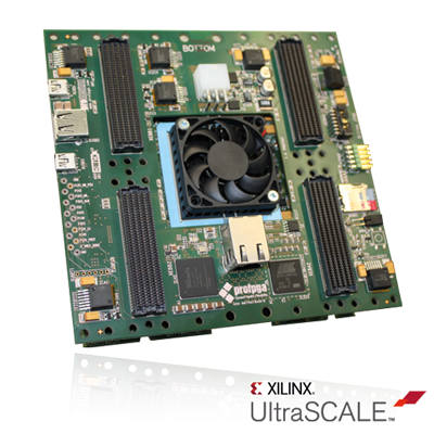
proFPGA uno VUS Prototyping System
Technical highlights on 440 Prototyping Board
- Handling up to 30 M ASIC gates capacity
- Modular supporting various proFPGA FPGA Modules
- Up to 1327 free user I/O
- Up to 10 individually adjustable voltage regions
- Up to 1.0 Gbps single ended point to point speed
ASIC Prototyping Solution
Product Summary
The proFPGA uno VUS 440 system is a complete and modular FPGA solution, which meets highest requirements in the area of FPGA based Prototyping. It addresses customers who need a scalable and flexible high speed ASIC Prototyping and IP verification solution for early software development and real time system verification. The innovative system concept offers highest flexibility and reusability, reconfigurability for several projects, which guarantees the best return on invest.
Highest Flexibility
The system architecture is based on a modular system concept. The FPGAs are assembled on dedicated FPGA modules, which will be plugged on the proFPGA uno, duo or quad motherboard. This offers the highest flexibility to use for example different FPGA types in one system. The user has nearly 100% access to all available I/Os of the FPGA, which gives him maximum freedom regarding the FPGA interconnection structure. This way the prototyping system can be adapted in the best way to any user design. Furthermore the system offers a total of 10 extension sites on the top and bottom site for stan- dard proFPGA or user specific extension boards like DDR-4 memory, PCIe gen1/2/3, Gigabit Ethernet, USB 3.0 or other high performance interface.
Maximum Performance
The well designed boards of the proFPGA system are optimized and trimmed to guarantee best signal integrity and to achieve highest performance. The high speed boards together with specific high speed connectors allow a maximum point to point speed of up to 1.0 Gbps single ended over the standard FPGA I/O and up to 12.5 Gbps differential over the high speed serial transceivers of the FPGA. This performance combined with the high interconnection flexibility allows the designer to run his design at maximum speed in the proFPGA system.
Big Capacity
Equipped with one Xilinx Virtex® UltraScale™ 440 FPGA module, the proFPGA uno system can handle up to 30 M ASIC gates on only one board.
Very User Friendly
The proFPGA prototyping system provides an extensive set of features and tools, like remote system configuration, integrated self and performance test, automatic board detection, automatic I/O voltage programming, system scan and safety mechanism, which simplifies the usage of the FPGA based system tremendously.
Specification
Available FPGA types
- Xilinx Virtex® XCVU440 FPGA Modules, or Xilinx Virtex® 7based FPGA modules
Capacity
- Up to 30 M ASIC gates on one board (Virtex® XCVU440 FPGA)
FPGA-internal memory
- Up to 88,600kbits kbits on one board (Virtex® XCVU440 FPGA)
Signaling rate
- Up to 10 Extension sites with high speed connectors
Extension sites
- Up to 88,600kbits kbits on one board (Virtex® XCVU440 FPGA)
I/O resources
- Overall up to 1327 signals for I/O and inter FPGA connection
- 1327 free I/Os per FPGA Module (Virtex® XCVU440 FPGA)
- 4x153 I/Os and 1x52 I/Os and 1x51 I/Os to top side connectors
- 4x153 I/Os to bottom side connectors
- Single-ended or differential
High Speed I/O transceivers
- 48 MGTs (up to 12.5 Gbps) (Virtex® XCVU440 FPGA)
- 16 MGTs (12.5 Gbps)(Virtex® XC7V2000T FPGA)
Voltage regions
- Up to 10 individually adjustable I/O voltage regions
- 10 individually adjustable voltage regions per FPGA Module (Virtex® XCVU440 FPGA)
- Stepless from 1.0V up to 1.8V on 9 extension sites, from 1.0V up to 3.3V on one extension site
- Automated detection of daughter card and adjustment of right voltage
Configuration
- With host software via Ethernet, USB 2.0 or standalone over USB stick
Clock Management
- 8 fixed clocks, 2 quartz as clock references
- Run-time configurable local clocks
- 8 global clock and sync signal inputs per motherboard
- Fully synchronous derived clocks with sync signals
System Architecture

Configurations
| proFPGA uno Xilinx Virtex® UltraScaleᵀᴹ 440 and V7 FPGA Prototyping System Configurations | ||||
| proFPGA uno VUS 440 | proFPGA uno V7 2000T | proFPGA uno V7 690T | proFPGA uno V7 585T | |
| Extension Sites | 10 | 8 | 8 | 8 |
| FPGA Modules | 1 | 1 | 1 | 1 |
| FPGAType | Xilinx Virtex® XCVU440 | Xilinx Virtex® XC7V2000T | Xilinx Virtex® XC7VX690T | Xilinx Virtex® XC7V585T |
| Logic Capacity (ASIC Gates) | 30 M | 12 M | 4.2 M | 3.5 M |
| FPGA Memory | 88,600 kbits | 46,512 kbits | 52,920 kbits | 28,620 kbits |
| I/O Resources | 1327 | 1084 | 738 | 738 |
| High Speed I/O Transceivers | 48 | 16 | 36 | 36 |
| Adjustable Voltage Regions | 10 | 8 | 8 | 8 |
| Clock Generators | 8 fixed clocks | 8 fixed clocks | 8 fixed clocks | 8 fixed clocks |
| Order Code | PROF-UNO-VUS-440 | PROF-UNO-V7-2000T | PROF-UNO-V7-690T | PROF-UNO-V7-585T |
Technologies
![]()
FPGA Mixing Technology (FMT)
- Easy plugging and unplugging of FPGA modules on motherboard
- Various FPGAs from different vendors can be used
- Automatic scanning and detection of FPGA modules, when plugged
- Different FPGA configurations are handled and controlled by profpga Messenger
![]()
Smart Stacking Technology (SST)
- Automatic Board detection when boards are plugged
- Automatic and right I/O voltage setting and programming with conflict detection
- Integrated interconnection self and performance test
- Smart I/O resource management. No I/O resources get lost or get blocked by connectors
![]()
Device Message Box Interface (DMBI)
- High speed, low latency data exchange system
- Enables various use modes like remote system configuration and monitoring and debugging
- Up to 4 Gbps data transfer rate
- Runs over USB or Ethernet
![]()
Advanced Clock Management (ACM)
- Run-time configurable local clocks. Fully synchronous derived clocks with sync signals.